General Description
The RTQ2118A provides the electrical signatures on D+/D- to support charging schemes compatible with the USB 2.0 Battery Charging Specification BC1.2 and Chinese Telecommunication Industry Standard YD/T 1591-2009. Auto-detect mode is also integrated which supports USB 2.0 Battery Charging Specification BC1.2 Dedicated Charging Port (DCP), Divider 3 mode and 1.2V shorted mode to comply with the legacy fast charging mode of mobile devices.
The RTQ2118A integrates a high efficiency, monolithic synchronous buck converter that can deliver up to 3A output current from a 3V to 36V wide range input supply and is protected from load-dump transients up to 42V.
Performance Specification Summary
The Automotive HV-Buck conveter has an input voltage range from 3V to 36V, and the output voltage is 5V. It can operate in forced PWM mode and PSM mode. And the current limit is implemented by RLIM for difference application. RTQ2118A is available in a WETD-VQFN-32L 5x5 package.
Table 1. RTQ2118A Evaluation Board Performance Specification Summary
|
Specification
|
Test Conditions
|
Min
|
Typ
|
Max
|
Unit
|
|
Input Voltage Range
|
|
3
|
--
|
36
|
V
|
|
Output Current
|
RLIM = 47kΩ
|
3.52
|
4
|
4.48
|
A
|
|
Default Output Voltage
|
Setting by the FB pin
|
--
|
5
|
--
|
V
|
|
Operation Frequency
|
Setting by the RT pin
|
300
|
--
|
2200
|
kHz
|
|
Output Ripple Voltage
|
VIN = 12V, VOUT = 5V, IOUT = 3A
|
--
|
20
|
--
|
mVp-p
|
|
Line Regulation
|
CCM, VIN = 6V to 19V, VOUT = 5V, IOUT = 2.4A
|
--
|
1
|
--
|
%
|
|
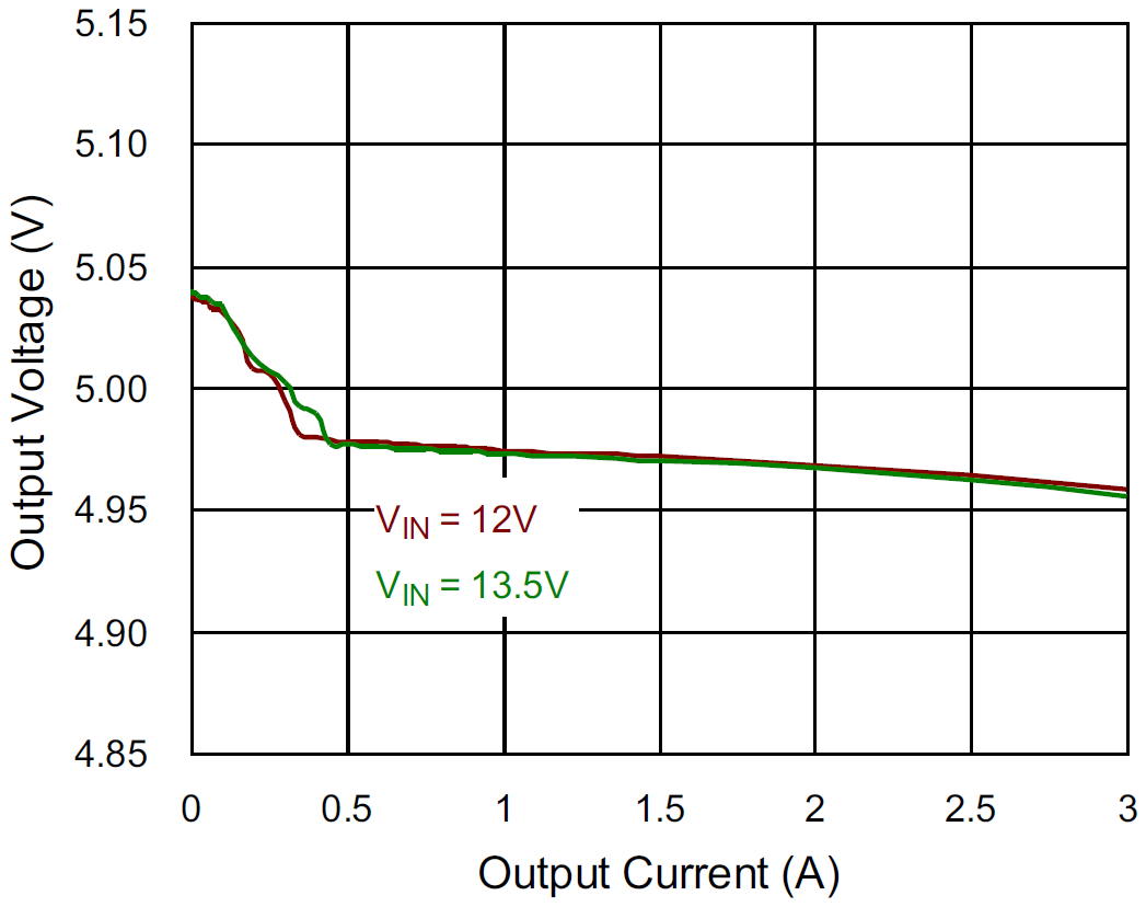
Load Regulation
|
CCM, VIN = 12V, VOUT = 5V, IOUT < 3A
|
--
|
1
|
--
|
%
|
|
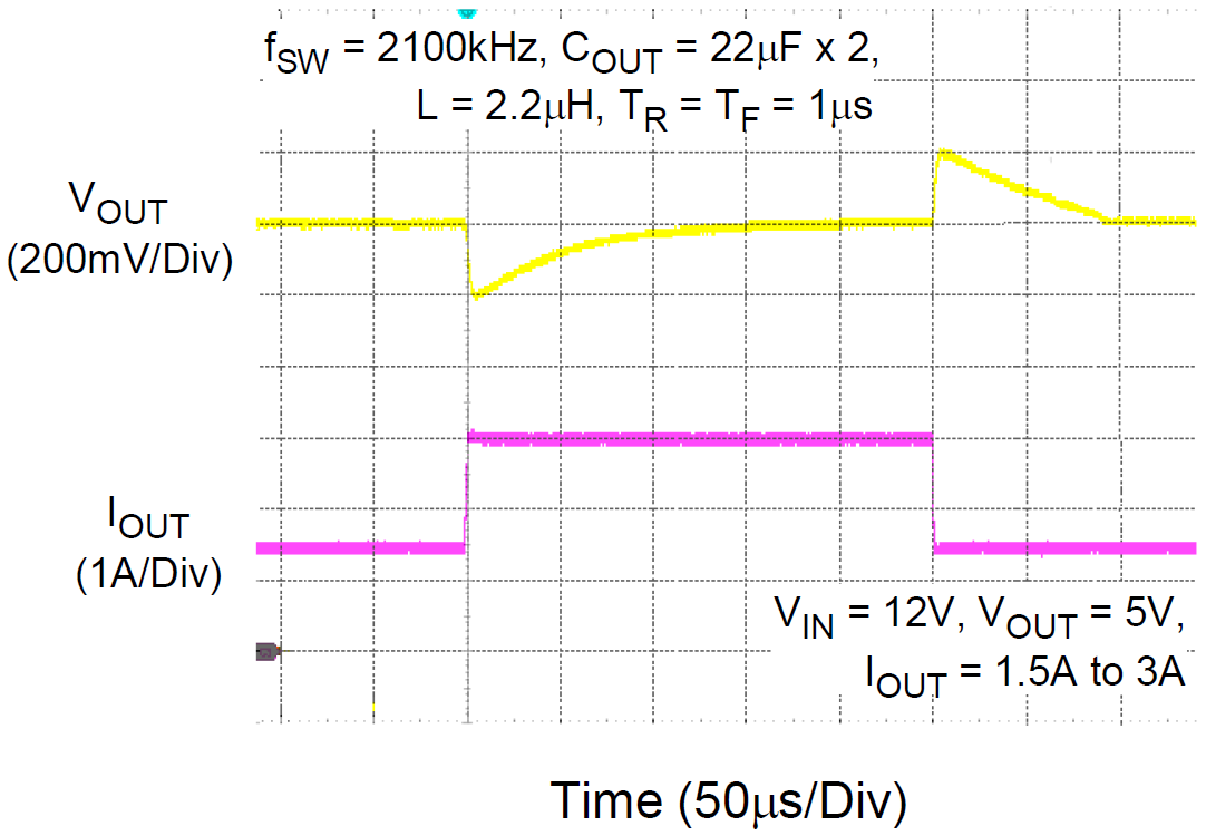
Load Transient Response
|
VIN = 12V, VOUT = 5V, IOUT = 1.5A to 3A
|
-5
|
--
|
5
|
%
|
|
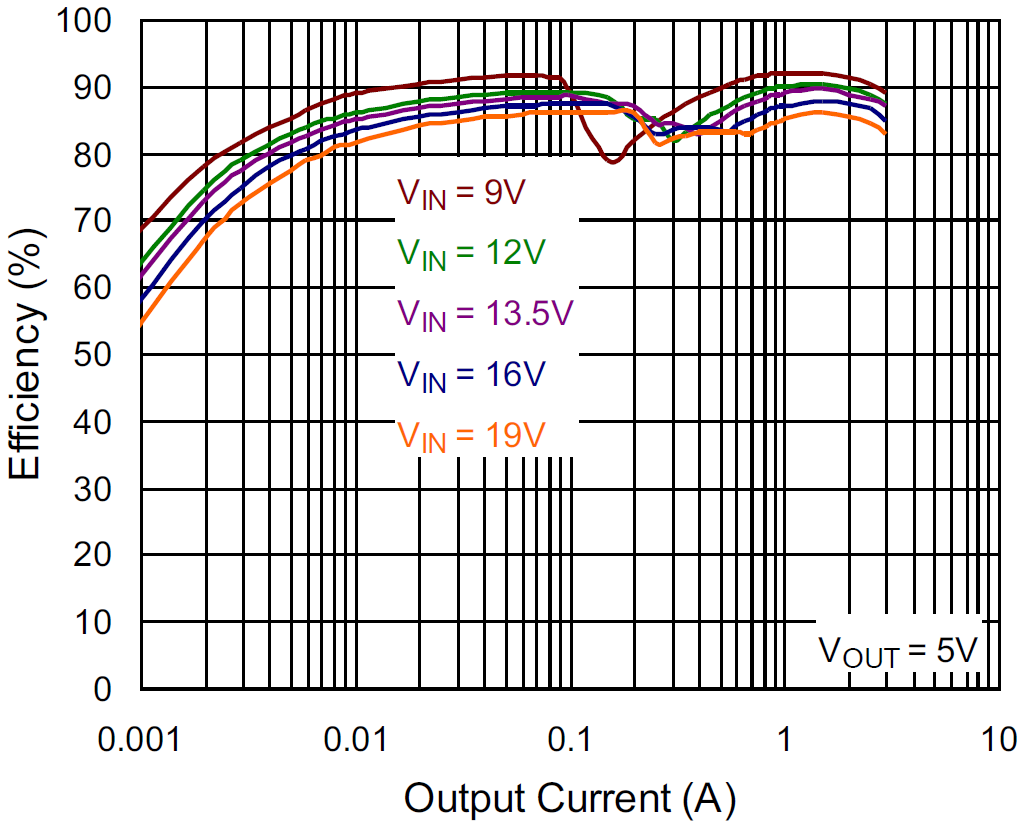
Maximum Efficiency
|
VIN = 9V to 19V, VOUT = 5V, IOUT = 0A to 3A
|
--
|
91
|
--
|
%
|
Power-up Procedure
1. Connect input voltage (3V < VIN < 36V) to the VIN pin.
2. Setting MODE and RLIM for device request.
3. To enable Buck converter by the external EN pin.
4. To connect an external load to output and verify the output voltage versus applied current.
Output Voltage Setting
The output voltage set by external feedback resistors expressed in the following equation.
where the reference voltage VFB is 0.8V (typical).
The placement of the resistive divider should be as close as possible to the FB pin. For better output voltage accuracy, the divider resistors with ±1% tolerance or better should be used. The resistance of R2 is not larger than 170kΩ for noise immunity considerationis recommended .
Detailed Description of Hardware
Headers Description and Placement
Carefully inspect all the components used in the EVB according to the following Bill of Materials table, and then make sure all the components are undamaged and correctly installed. If there is any missing or damaged component, which may occur during transportation, please contact our distributors or e-mail us at evb_service@richtek.com.
Test Points
The EVB is provided with the test points and pin names listed in the table below.
|
Test Point/
Pin Name
|
Function
|
|
VIN
|
Input voltage
|
|
VBUS
|
Output voltage
|
|
SW
|
Switching node
|
|
GND
|
GND
|
|
DS+
|
Data line
|
|
DS-
|
Data line
|
|
CC1
|
Type-C configuration pin
|
|
CC2
|
Type-C configuration pin
|
Bill of Materials
|
Reference
|
Count
|
Part Number
|
Description
|
Package
|
Manufacturer
|
|
U1
|
1
|
RTQ2118AGQVT-QA
|
USB Type-C and Power Delivery
|
WETD-VQFN-32L 5x5
|
RICHTEK
|
|
C1, C2
|
2
|
GRM31CR61H106KA12L
|
10μF/50V/X7R
|
1210
|
Murata
|
|
C3, C8, CBOOT
|
3
|
C1608X7R1H104K080AA
|
100nF/50V/X7R
|
0603
|
TDK
|
|
C5, C6
|
2
|
CL31A226KAHNNE
|
22μF/25V/X5R
|
1210
|
SAMSUNG
|
|
CVCC
|
1
|
C2012X7R1A106K125AC
|
1μF/10V/X7R
|
0805
|
TDK
|
|
CSS
|
1
|
C1608X7R1H103K080AA
|
10nF/50V/X7R
|
0603
|
TDK
|
|
CCOMP1
|
1
|
0603B472K500CT
|
4.7nF/50V/X7R
|
0603
|
WALSIN
|
|
L1
|
1
|
1217AS-H_2R2N=P3
|
2.2μH/9.3A (Maximum)
|
8.0x8.0x4.5mm
|
Murata
|
|
J1
|
1
|
UAF-041RGPB-CF1066
|
USB Type-A
|
USB-4P-DIP-AL
|
Cherng Weei
|
|
R0, RBOOT
|
2
|
WR06X000 PTL
|
0
|
0603
|
WALSIN
|
|
R1
|
1
|
RTT031053FTP
|
105k
|
0603
|
RALEC
|
|
R2
|
1
|
RTT032002FTP
|
20k
|
0603
|
RALEC
|
|
R21
|
1
|
WR08X2000FTL
|
200
|
0805
|
WALSIN
|
|
R46, R47
|
2
|
RTT031001FTP
|
1k
|
0603
|
RALEC
|
|
R55
|
1
|
WR06X1002FTL
|
10k
|
0603
|
WALSIN
|
|
R56, REN, RMODE/ SYNC, RPG
|
4
|
WR06X1003FTL
|
100k
|
0603
|
WALSIN
|
|
R210
|
1
|
WR04X000 PTL
|
0
|
0402
|
WALSIN
|
|
RCS1, RCS2
|
2
|
TGL120610FR060P05Z
|
0.06
|
1206
|
EVER OHMS
|
|
RCS3
|
1
|
RTT062R00FTP
|
short
|
1206
|
RALEC
|
|
RRLIM
|
1
|
RTT033302FTP
|
33k
|
0603
|
RALEC
|
|
RRT
|
1
|
WR06X2202FTL
|
22k
|
0603
|
WALSIN
|
|
RCOMP
|
1
|
RTT037681FTP
|
7.68k
|
0603
|
RALEC
|
|
USB3
|
1
|
UP2-AH-1-T
|
USB Type-A
|
12.75x18.75x5.52mm
|
CUI Devices
|
Typical Applications
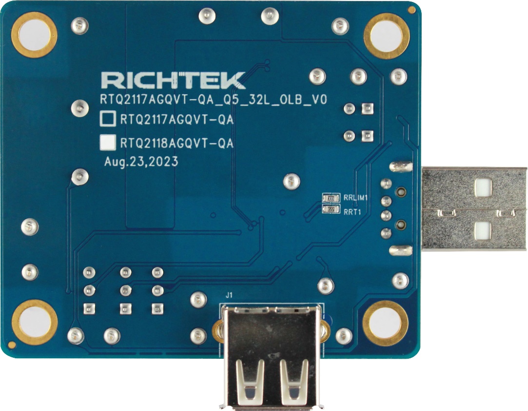
EVB Schematic Diagram
1. The capacitance values of the input and output capacitors will influence the input and output voltage ripple.
2. MLCC capacitors have degrading capacitance at DC bias voltage, and especially smaller size MLCC capacitors will have much lower capacitance.
Measure Result
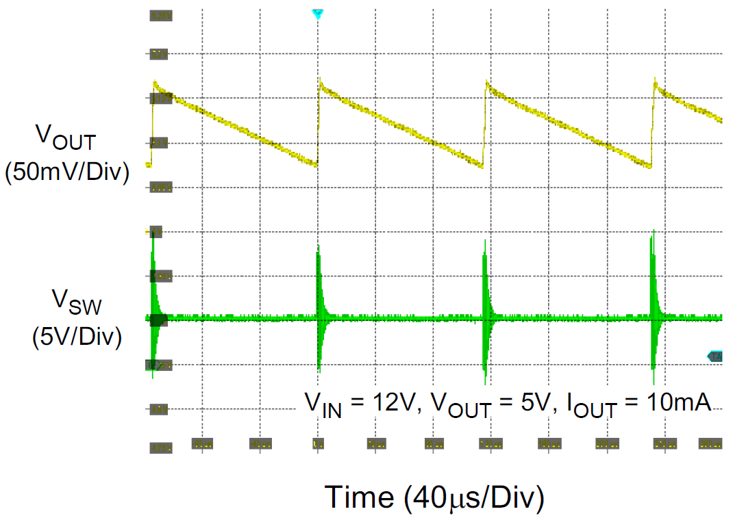
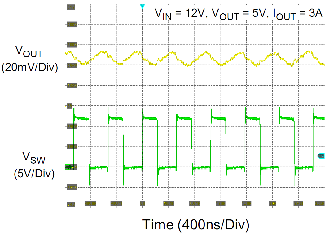
|
Output Ripple Measurement
|
Output Ripple Measurement
|
|
|
|
|
Load Transient Response
|
Output Voltage vs. Output Current
|
|
|
|
|
Efficiency vs. Output Current
|
|
|
Note: When measuring the input or output voltage ripple, care must be taken to avoid a long ground lead on the oscilloscope probe. Measure the output voltage ripple by touching the probe tip directly across the output capacitor.
Evaluation Board Layout
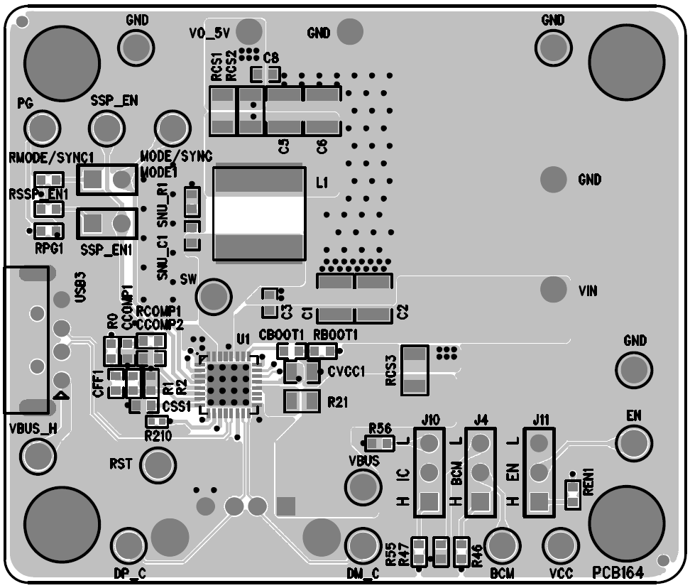
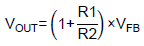
Figure 1. Top View (1st layer)

Figure 2. PCB Layout—Inner Side (2nd Layer)

Figure 3. PCB Layout—Inner Side (3rd Layer)
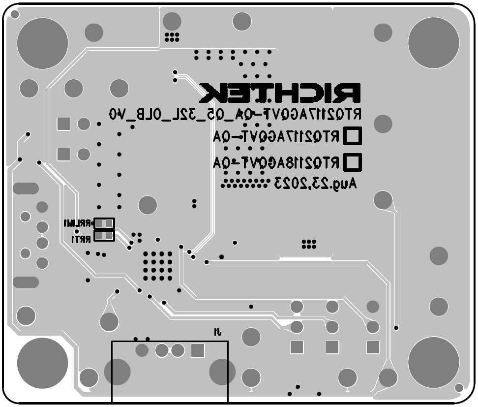
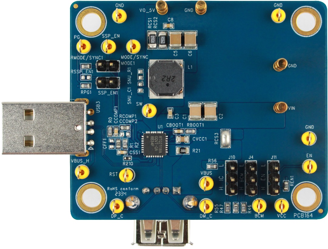
Figure 4. Bottom View (4th Layer)